NCP1606
http://onsemi.com
16
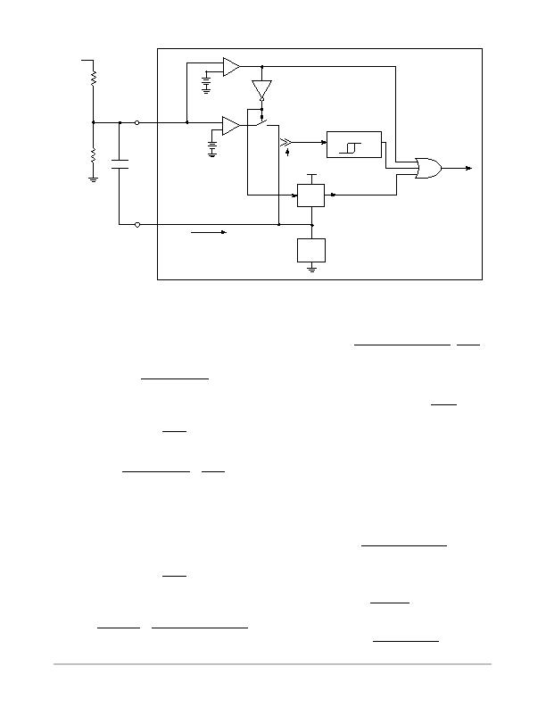
Figure 34. OVP and UVP Circuit Blocks
FB
Control
+
E/A
+
Measure
300 mV
2.5 V
UVP
Fault
Dynamic OVP
V
EAH
Clamp
Static OVP is triggered
when clamp is activated.
V
EAL
Clamp
Static OVP
Enable
(Enable EA)
R
OUT2
R
OUT1
C
COMP
V
DD
I
CONTROL
> I
ovp
V
OUT
I
CONTROL
V
CONTROL
I
CONTROL
When the output voltage is in steady state, R
OUT1
and
R
OUT2
regulate the FB voltage to 2.5 V. Also, during this
equilibrium state, no current flows through the
compensation capacitor (
C
COMP
of Figure 1). Therefore:
" The R
OUT1
current is:
I
R
OUT1
+
(V
OUT
)
nom
* 2.5 V
R
OUT1
(eq. 6)
where (V
OUT
)
nom
is the nominal output voltage.
" The R
OUT2
current is:
I
R
OUT2
+
2.5 V
R
OUT2
(eq. 7)
" And since no current flows through C
COMP
,
I
R
OUT1
+I
R
OUT2
?/DIV>
(V
OUT
)
nom
* 2.5 V
R
OUT1
+
2.5 V
R
OUT2
(eq. 8)
Under stable conditions, these equations are true.
Conversely when V
OUT
is not at its nominal level, the
output of the error amplifier sinks or sources the current
necessary to maintain 2.5 V on pin 1. In particular, in the
case of an overvoltage condition:
" The error amplifier maintains 2.5 V on pin 1, and the
R
OUT2
current remains:
I
R
OUT2
+
2.5 V
R
OUT2
(eq. 9)
" The R
OUT1
current is:
I
R
OUT1
+
V
OUT
2.5 V
R
OUT1
+
(V
OUT
)
nom
) DV
OUT
2.5 V
R
OUT1
(eq. 10)
where DV
OUT
is the output voltage excess.
" Therefore, the error amplifier sinks:
I
R
OUT1
I
R
OUT2
+
(V
OUT
)
nom
) DV
OUT
2.5 V
R
OUT1
2.5 V
R
OUT2
(eq. 11)
The combination of Equations 2 and 11 leads to a very
simple expression of the current sunk by the error
amplifier:
I
CONTROL
+ I
R
OUT1
* I
R
OUT2
+
DV
OUT
R
OUT1
(eq. 12)
Hence, the current absorbed by pin 2 (I
CONTROL
) is
proportional to the output voltage excess. The circuit
senses this current and disables the drive (pin 7) when
I
CONTROL
exceeds I
OVP
(typically 40 mA in NCP1606A,
10.4 mA in NCP1606B). This gives the OVP threshold as:
(V
OUT
)
OVP
+ (V
OUT
)
nom
) (R
OUT1
@ I
OVP
)
By simply adjusting R
OUT1
, the OVP limit can be easily
set. Therefore, one can compute the R
OUT1
and R
OUT2
resistances using the following procedure:
1. Select R
OUT1
to set the desired overvoltage level:
R
OUT1
+
(V
OUT
)
OVP
* (V
OUT
)
nom
I
OVP
For instance if implementing the NCP1606B, and
420 V is the maximum output level and 400 V is the
nominal output level, then
R
OUT1
+
420 * 400
10.4 mA
+ 1.9 MW
2. Select R
OUT2
to adjust the regulation level:
R
OUT2
+
2.5 V @ R
OUT1
V
OUT(nom)
* 2.5 V
发布紧急采购,3分钟左右您将得到回复。
相关PDF资料
NCP1607BDR2G
IC PFC CONTROLLER CRM 8SOIC
NCP1611BDR2G
IC PFC CTLR HE ENHANCED 8-SOIC
NCP1651DR2G
IC PFC CONTROLLER CCM/DCM 16SOIC
NCP1654BD133R2G
IC PFC CCM 133KHZ 8-SOIC
NCP1927DR2G
IC CTLR PFC/FLYBACK 16-SOIC
NCP380HMU21AATBG
IC CURRENT LIMIT SWITCH 6-UDFN
NCT1008DMT3R2G
TMP DIO MON/SMBUS 4CH 8WDFN
NCT210RQR2G
IC TEMP SENSOR LOC/REM 16QSOP
相关代理商/技术参数
NCP1606BOOSTGEVB
功能描述:电源管理IC开发工具 OSPI NCP1606 100 W BOOST
RoHS:否 制造商:Maxim Integrated 产品:Evaluation Kits 类型:Battery Management 工具用于评估:MAX17710GB 输入电压: 输出电压:1.8 V
NCP1606BPG
功能描述:功率因数校正 IC LO CST PWR FCTR CONT RoHS:否 制造商:Fairchild Semiconductor 开关频率:300 KHz 最大功率耗散: 最大工作温度:+ 125 C 安装风格:SMD/SMT 封装 / 箱体:SOIC-8 封装:Reel
NCP1607BDR2G
功能描述:功率因数校正 IC CST EFCT PW FCTR CTR RoHS:否 制造商:Fairchild Semiconductor 开关频率:300 KHz 最大功率耗散: 最大工作温度:+ 125 C 安装风格:SMD/SMT 封装 / 箱体:SOIC-8 封装:Reel
NCP1607BOOSTGEVB
功能描述:BOARD EVAL NCP1607 100W BOOST RoHS:是 类别:编程器,开发系统 >> 评估演示板和套件 系列:* 标准包装:1 系列:PCI Express® (PCIe) 主要目的:接口,收发器,PCI Express 嵌入式:- 已用 IC / 零件:DS80PCI800 主要属性:- 次要属性:- 已供物品:板
NCP1608BDR2G
功能描述:功率因数校正 IC COST EFFECT PWR FACT CONT RoHS:否 制造商:Fairchild Semiconductor 开关频率:300 KHz 最大功率耗散: 最大工作温度:+ 125 C 安装风格:SMD/SMT 封装 / 箱体:SOIC-8 封装:Reel
NCP1608BOOSTGEVB
功能描述:电源管理IC开发工具 NCP1608 100 W BOOST EVB PWR SPY
RoHS:否 制造商:Maxim Integrated 产品:Evaluation Kits 类型:Battery Management 工具用于评估:MAX17710GB 输入电压: 输出电压:1.8 V
NCP1611ADR2G
功能描述:功率因数校正 IC NCP1611A ENHANCED PFC
RoHS:否 制造商:Fairchild Semiconductor 开关频率:300 KHz 最大功率耗散: 最大工作温度:+ 125 C 安装风格:SMD/SMT 封装 / 箱体:SOIC-8 封装:Reel
NCP1611BDR2G
功能描述:功率因数校正 IC NCP1611A ENHANCED PFC RoHS:否 制造商:Fairchild Semiconductor 开关频率:300 KHz 最大功率耗散: 最大工作温度:+ 125 C 安装风格:SMD/SMT 封装 / 箱体:SOIC-8 封装:Reel